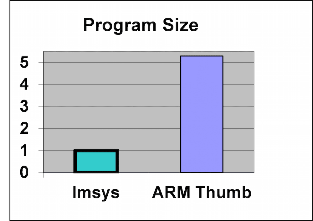
Due to the “Utilization Wall,” future CMOS technology calls for a radically new microprocessor architecture with less transistor switching, to take full advantage of both density and speed.
This is important not only for big many-core processors but also very small chips that are to be made in very large quantities, such as many of the nodes in the Internet of Things (IoT).
A novel processor architecture, having built-in support for LLVM, has been developed by Imsys. A proof-of-concept chip has been manufactured in 65nm. Measurements verify that performance is comparable to that of much bigger processor cores, and that energy efficiency is better than what has been reported for architectures claimed to be the most efficient.
The chip includes Imsys’ patented dual core solution. Its pair of independent cores occupies 40 % less space than two single cores, because it is dominated by shared microcode. The cores also share memories for program and data. Current consumption is 18 mA at 1.2V and 350 MHz with both cores active.
The chip demonstrates the solution both as a microcontroller for IoT nodes and as a cell for many-core designs, and therefore contains a five port grid network router (NOC). Hundreds of such independent general-purpose cells, each with local memory for code and data sufficient for the threads they execute, can be integrated on a 65nm die; thousands if state-of-the-art technology is used.
The design uses a compact flexible logic core and extensive microprogramming to accomplish a rich set of operations created directly for the compilers. This reduces
• the number of program bytes to fetch (i.e. cost and energy consumption in memory)
• the number of transistors in the logic core (i.e. its cost)
• the number of transistor switching events per source-code line (i.e. energy consumption per task).
This is very different from computer processors, which have a long history of using what was then “free” transistors for performance improvements, now increasingly irrelevant but still dominating their cores.
A rich LLVM Bitcode-like instruction set has been developed and produces higher code density than any of the well-known architectures do. Apple is heavily supporting the use of LLVM and has decided that all development for iWatch shall use the iWatch SDK from day one.
The many-core application will need special functionality for efficient inter-cell communication. This is accomplished by dedicated microcode without added hardware logic. Similarly, such applications may need 64bit addressing, which requires only modest changes to the microcode for the LLVM operations – the needed hardware resources for the extended address are already there.
Imsys processors routinely switch dynamically between instruction sets, totally defined by microcode. The processor is runtime reconfigurable and new instruction can be added at any time. Optimizing crypto functions resulted in a performance gain of between 2.7 and 43 times compared with C code. Peripheral functionality like Ethernet, crypto/security, sigmadelta A/D conversion, graphics, media processing, and camera/display input/output has been microprogrammed and don’t require dedicated hardware logic.
-
Awards
-
 2015 Top 100 Entries
Like this entry?
-
About the Entrant
- Name:Roger Sundman
- Type of entry:teamTeam members:Stefan Blixt
Ning Ma
David Juhasz
Zhuo Zou - Software used for this entry:LLVM
- Patent status:patented


