Welding technologies are fundamental to fabrication and ubiquitous within manufacturing. Laser welding has found wide application for the joining of precision metal components and high-speed production due to the intense laser heat source. Low penetration or “conduction mode” welding is well controlled, depositing energy and melting at the surface of the metal. However, deep penetration laser welding relies on “keyhole melting,” the formation of an unstable vapor cavity that may be the source for defects such as porosity, voids, ejecta, vaporization and cracking.
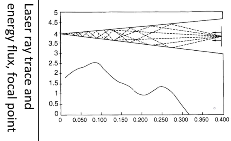
A multiphysics approach can design weld joints that function as non-imaging optical concentrators to efficiently capture, direct and concentrate laser energy by multiple reflections and absorption to produce melting, flow and coalescence while avoiding detrimental vaporization, spatter, ejecta and plasma formation within the keyhole. This design both reduces pressure buildup and prevents keyhole collapse.
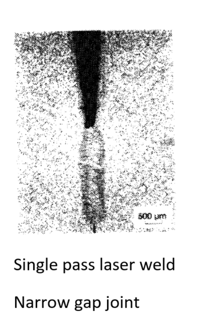
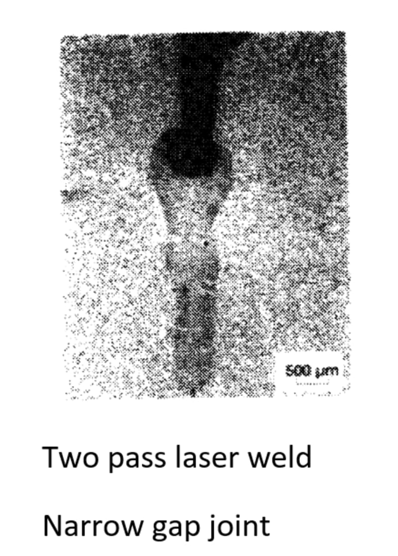
This approach extends the work of previous inventions that relied only on CAD design and optical ray tracing, to combine full 3D Multiphysics modeling using COMSOL. Ray tracing, melting, fluid flow, solidification, metallurgical transformation, thermal and mechanical responses are combined into a single application. Previous work (USPTO Patents - 5760365, 6917010, 6300591) demonstrated the proof of principal with prototypical welds, multi-pass autogenous welding, laser welding of copper, precision laser brazing and replacing the environmental burden of soldering when fabricating solar collector hardware.
These innovative designs will enable deep defect free welds using less energy allowing the use of lower cost lasers. This approach could replace arc seam welding requiring significantly less material removal during joint preparation while enabling significantly higher speeds. In addition, COMSOL multi-physics simulation apps may be used to generate digital twins and populate datasets for use by machine learning, control systems and to specify acceptance ranges for all conditions.
These designs are novel as they design and incorporate an easily manufactured optical element within the components to be welded and create no additional fabrication penalty for precision machined components. Alternatively, a seam tracking system may be used to prepare the narrow gap joint geometry and could be integrated into the automated welding sequence. Multiphysics models for a family of applications and materials may be calibrated using easy to obtain weld cross section data.
The weld multiphysics based joint design COMSOL app is the monetized product. This methodology will see wide application extending the large market for welding thicker section products and for automated, autonomous and remote operations. Applications will serve the aerospace, automotive, transportation, and energy sectors requiring precision welding.
In example, current efforts to build reusable spacecraft using arc welding can create distortion and buckling leading to variations in weld penetration and reducing performance under cryogenic and pressurized application. This method will improve fabrication of welded hardware on earth, in orbit, on the moon and beyond. These applications will save both time, money, create and lead manufacturing into the future.
-
Awards
-
 2020 Top 100 Entries
Like this entry?
-
About the Entrant
- Name:John Milewski
- Type of entry:teamTeam members:John O. Milewski, APEX3D LLC, Santa Fe NM
Cormac F. McCabe, Ben Franklin Academy, Druid Hills GA - Software used for this entry:OptiCAD, COMSOL, Fusion 360
- Patent status:none


